


Key Takeaways
- Columbia Engineering researchers have developed a method to create 3D electronic devices using DNA self-assembly.
- This new technique may enhance computing power and aid in developing AI systems inspired by the brain’s structure.
- The process is scalable, allowing for thousands of devices to be manufactured simultaneously on silicon wafers.
Dramatic Shift in Electronics Manufacturing
Researchers at Columbia Engineering, led by Professor Oleg Gang, have achieved a significant milestone by using DNA to construct 3D functional electronic devices with nanometer-sized features. This innovative method marks a departure from traditional 2D electronics, suggesting that moving to a 3D architecture can increase the density and computing power of electronic devices. The findings were published in the journal Science Advances.
Professor Gang highlights that 3D electronic structures mimicking the brain’s natural architecture could vastly improve the performance of brain-inspired AI systems compared to current 2D designs. The new bottom-up manufacturing technique not only presents a solution to the challenges posed by conventional top-down fabrication methods but also offers scalability, enabling the creation of thousands of devices in parallel.
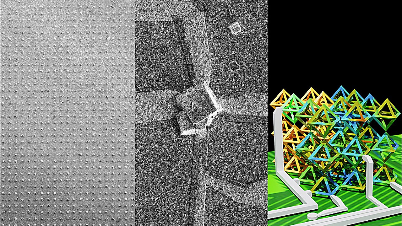
Current electronics are typically built through top-down approaches, where material is sequentially removed to create desired structures. This method, likened to sculpting, often struggles to accurately produce complex 3D designs and is susceptible to cumulative errors over lengthy production processes. To address this, Gang’s team has introduced a biologically inspired approach that utilizes the self-assembly property of DNA, where strands can fold into specific shapes, forming intricate 3D frameworks at the nanoscale.
DNA consists of four types of molecules represented by the letters A, T, C, and G, which pair in specific combinations (A with T, and C with G). By designing various sequences, researchers can engineer DNA strands to fold into 2D and 3D structures. These structures, held in place by additional DNA snippets, serve as building blocks for larger frameworks.
In their study, the researchers created gold square arrays as substrates for attaching short DNA strands that act as anchors for octahedral DNA frames, which self-assemble into 3D scaffolds at predetermined locations. This carefully designed setup facilitates the growth of 3D structures in specific patterns on silicon wafers.
The team, in collaboration with the University of Minnesota, further advanced their prototype by coating these DNA scaffolds with silicon oxide, integrating semiconductor tin oxide, and attaching electrodes. The result is a functional light sensor that generates an electrical response upon illumination, indicating successful integration of 3D structures into microchips.
Gang expressed enthusiasm about transforming futuristic concepts into operational devices through this bottom-up approach. The scalable manufacturing process opens the potential for producing complex 3D electronic devices in a cost-effective manner.
Looking ahead, the research team aims to expand this methodology to develop even more sophisticated electronic technologies that involve multiple materials, with a vision of creating advanced 3D circuitry for the future.
The content above is a summary. For more details, see the source article.


