


Key Takeaways
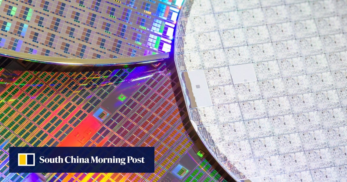
- Chinese researchers have created the world’s largest N-polar gallium nitride (GaN) wafer, measuring eight inches.
- This innovation could reduce semiconductor production costs by 40%, enhancing the technology’s adoption in sectors like satellite communications and electric vehicles.
- N-polar GaN wafers offer superior performance, with the new fabrication technique eliminating previous size and cost limitations.
Breakthrough in Semiconductor Technology
Chinese researchers have announced a significant advancement in semiconductor technology with the development of the world’s largest N-polar gallium nitride (GaN) wafer, measuring eight inches (20.3 cm). This breakthrough is expected to reduce production costs by 40%, facilitating the rapid adoption of GaN technology in key areas such as satellite communications and electric vehicles (EVs).
GaN is recognized as a leading third-generation compound semiconductor, transforming high-frequency and high-power applications, including 5G and 6G networks, satellite communications, autonomous vehicles, and advanced radar systems. Its superior physical properties have already allowed for innovations such as palm-sized 100W fast chargers, minimized energy conversion losses in 800V EV platforms to below 5%, and a tripling of satellite communication bandwidth.
Industry analysts anticipate that GaN’s mass production could lead to dramatic changes across these sectors, particularly as the technology matures. Central to GaN’s capabilities is its crystal polarity. While both nitrogen-polar (N-polar) and gallium-polar (Ga-polar) versions exist, N-polar GaN typically exhibits better performance. However, stringent growth requirements and complex production methods have previously restricted global output to small batches of two to four-inch N-polar GaN wafers at high costs.
On March 22, a research team at the JFS Laboratory in Wuhan, Hubei province, successfully fabricated the first-ever eight-inch N-polar GaN-on-insulator (GaNOI) wafers on a silicon substrate. This innovation disrupts existing technological monopolies and significantly lowers wafer costs while enhancing the device breakdown voltage to 2000V.
The implications of this breakthrough are far-reaching, offering a more accessible and cost-effective path to incorporating high-performance GaN technology into various applications, which could transform industries from telecommunications to electric mobility. With this development, the semiconductor landscape is set for a potential reshaping, facilitating a more rapid roll-out of advanced technologies reliant on GaN.
The content above is a summary. For more details, see the source article.


