


Key Takeaways
- Boise State University researchers developed an environmentally friendly method for manufacturing flexible hybrid circuits using laser-induced graphene.
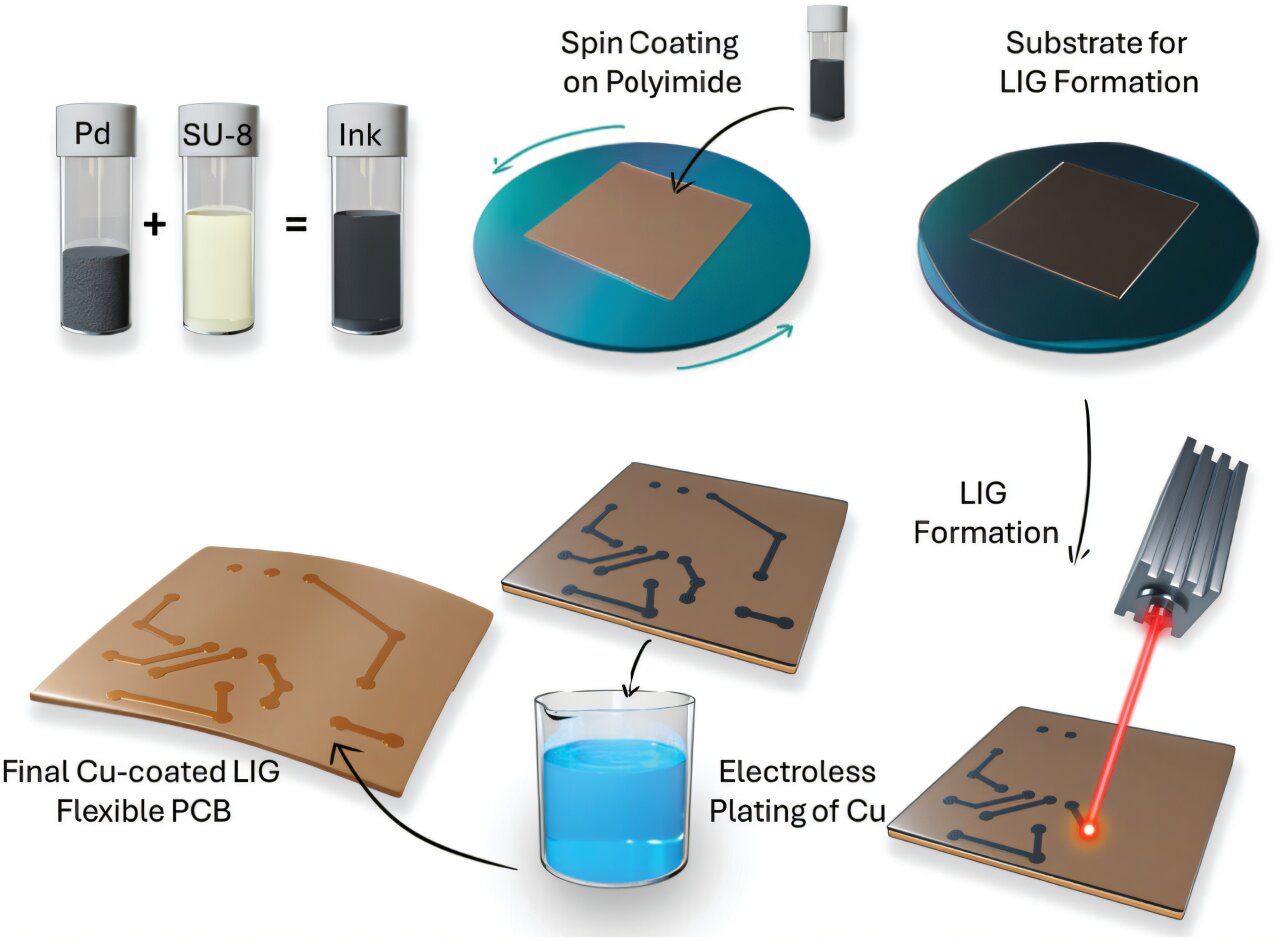
- The new technique incorporates palladium nanoparticles for copper interconnects, reducing waste and costs in printed circuit board production.
- The global demand for flexible PCBs is driving growth in the PCB market, projected to exceed $150 billion USD in the next decade.
Innovative Approach to Circuit Manufacturing
Researchers at Boise State University have introduced an advanced method for creating flexible hybrid circuits that emphasizes sustainability and cost-effectiveness. This innovative approach recently graced the cover of Advanced Materials Technologies.
The process employs laser-induced graphene (LIG), which transforms carbon-rich materials into a three-dimensional, conductive, and porous structure. This scalable and patternable technique is well-suited for various applications in electronics, sensing, and energy storage.
In their research, the team utilized palladium (Pd) nanoparticles incorporated into a polymer matrix to create Pd-functionalized laser-induced graphene. These nanoparticles serve as seed crystals facilitating the electroless deposition of copper onto the LIG framework, effectively forming copper interconnects ideal for flexible printed circuit boards (f-PCBs). The use of a laser-enabled additive manufacturing process enables these interconnects to integrate with discrete microelectronic components, resulting in a flexible hybrid operational amplifier capable of sensing resistance changes while undergoing bending. This capability underscores the diverse applications of this technology in sensing.
Lead author Attila Rektor noted the environmental benefits of their method, stating, "Additive manufacturing of printed circuit boards can help advance electronics manufacturing by reducing waste, cutting costs, and enabling rapid prototyping." This approach mitigates the use of harmful chemicals and excessive material waste, promoting a more sustainable PCB fabrication process.
The global printed circuit board (PCB) market is currently valued at approximately $90 billion USD, with predictions that it will surpass $150 billion USD over the next ten years. A significant factor driving this growth is the rising demand for flexible PCBs, known for their compact designs, reduced weight, and enhanced durability, particularly in wearable Internet of Things (IoT) applications.
Professor David Estrada from the Micron School of Materials Science and Engineering praised Rektor’s accomplishment, stating, "I was thrilled to hear that Attila’s work was recognized with the cover of Advanced Materials Technologies. His research not only bridges scientific discovery to practical applications but also introduces an innovative approach to manufacturing flexible PCBs—reducing costs and environmental impact by eliminating waste and harmful etching processes for our industrial partners."
This breakthrough signals a significant advancement in PCB manufacturing, aligning with global trends towards sustainability and efficiency. The research may pave the way for more eco-friendly electronics solutions, catering to the evolving demands of the market while addressing environmental concerns.
The content above is a summary. For more details, see the source article.


