


Key Takeaways
- Specialty devices, such as SiC and GaN power components, are integral across various industries, including automotive and telecommunications.
- A transition to larger wafer sizes (up to 300mm) is occurring, posing new challenges and requiring advanced manufacturing solutions.
- Innovations in specialty device manufacturing are essential for meeting the rising demand and complexity in sectors like consumer electronics and high-performance computing.
Expansion of Specialty Devices
Specialty devices, once considered a niche segment within the semiconductor industry, are gaining significant attention thanks to their varied applications in modern technology. The spotlight has primarily been on Silicon Carbide (SiC) and Gallium Nitride (GaN) power devices, which are becoming essential elements in automotive, green energy, fast-charge consumer electronics (CE), and high-performance computing (HPC) applications.
However, the realm of specialty devices extends beyond power solutions. These components encompass a wide range of functions, including microelectromechanical systems (MEMS) used in automobiles and consumer electronics, along with radio frequency (RF) filters crucial for 5G and 6G communications. Notably, photonics technology, once overlooked, is now making strides in areas like 3D sensing for consumer electronics and advanced driver assistance systems (ADAS) in vehicles.
The Promise of Photonics
Photonics, which facilitate remarkable optical communication opportunities, are poised to become game-changers. The most promising application appears to be co-packaged optics (CPO), a development that allows for direct optical communications from packaged XPU devices—a vital capability for artificial intelligence applications.
The Shift to Larger Wafer Sizes
Traditionally, specialty devices have utilized 150mm or 200mm wafers. However, advancements are driving a shift toward larger sizes. For instance, GaN devices are transitioning from 200mm to 300mm, while SiC devices are upgrading from 150mm to 200mm. This transition is crucial as it will enhance high-volume manufacturing capabilities and meet the increasing demand across various tech sectors.
This move, however, brings prominent challenges; specialty devices often require unique manufacturing processes and materials that demand customized inspection and metrology solutions.
Challenges in Manufacturing Specialty Devices
While transitioning to larger wafers can facilitate enhanced production, it introduces complex challenges specific to each specialty device type:
-
MEMS: Enhanced size and material diversity necessitate tighter process controls regarding etch depth and feature heights across warped substrates.
-
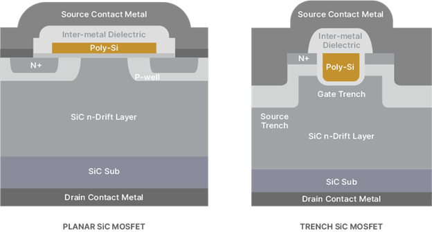
SiC Power: Moving to 200mm requires expanding inspection methods to account for increased crystal defects without affecting manufacturing throughput.
-
GaN Power: Transitioning to 300mm wafers results in variations that demand an increase in measurement points and exceptional control capabilities to maintain performance consistency.
-
Photonics and CPO: Co-packaged optics necessitate precise metrology tools designed for various bonding and alignment requirements.
-
CMOS Image Sensors (CIS): Elevated die counts and wafer diameters require advanced metrology to ensure uniformity and consistency, highlighting the need for upgraded inspection tools.
Manufacturers must adopt newer metrology and inspection technologies to navigate these challenges effectively. Suppliers with expertise in specialty technologies will be essential in meeting the industry’s evolving requirements for wafer handling, materials, and production efficiency.
The ongoing evolution of specialty devices reflects a growing market fueled by rising demands for greater functionality in established sectors like consumer electronics and automotive industries. Continued innovations will play a pivotal role in sustaining the momentum of this important technological segment.
The content above is a summary. For more details, see the source article.


