


Key Takeaways
- Backside power delivery networks (BPDNs) improve performance and reduce power losses but introduce new manufacturing challenges.
- Major semiconductor companies like Intel, Samsung, and TSMC are adopting BPDNs in their next-generation technologies, particularly at the 2nm node.
- New methods are required for thermal management and alignment control to address the challenges posed by BPDNs.
Backside power delivery networks (BPDNs) are poised to transform semiconductor manufacturing by enhancing processor performance while significantly improving efficiency. This architectural innovation repositions power delivery from the frontside of the chip to the backside, resolving issues like high voltage drop (IR drop) that have plagued advanced nodes. Notably, leading firms are making strides in implementing BPDNs alongside the shift towards nanosheet transistors.
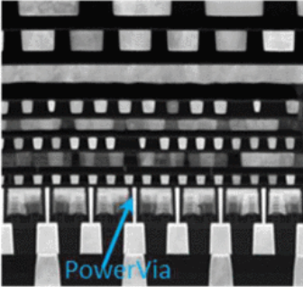
Intel has launched its 18A process, featuring its RibbonFET transistors and PowerVia technology. Samsung, an early adopter of gate-all-around (GAA) technology, plans to integrate backside power at its 2nm node, while TSMC is set to introduce GAA alongside its 16Å node (A16). The primary advantage of integrating BPDNs is a potential voltage drop reduction of up to 30% and thus improved power integrity.
The process entails removing substantial portions of the silicon wafer and aligning nano-silicon vias (nanoTSVs) with transistor connections, which necessitates innovative modeling to manage the increased heat generated by closely packed transistors. With a BPDN, the normalized thermal conditions may worsen, leading to potential hotspots within densely packed chip designs. Industry experts predict that localized thermal penalties can increase by as much as 14°C compared to traditional front-side power delivery networks.
BPDNs allow for segregated power and signal wiring, easing routing congestion on the frontside, which is critical for high-speed applications. This separation leads to improved area utilization and can enhance cell density for memory elements. However, effective implementation requires advanced manufacturing techniques, including precise wafer thinning, bonding processes, and lithography controls.
Nonetheless, challenges persist. Achieving fine alignment between backside power and frontside transistors is crucial and necessitates robust overlay control. The reduction of the silicon substrate can impair heat dissipation, requiring advanced materials and cooling methods to mitigate thermal resistance in chip designs. Innovative modeling techniques, including machine-learning algorithms, are being developed to better predict thermal performance amidst complex layouts.
As the industry moves towards direct connect implementations, where nanoTSVs contact transistor sources and drains directly, the tolerances for alignment become incredibly tight, presenting further technical hurdles. The productivity and performance benefits of BPDNs are expected to outweigh their complexities, particularly in high-performance computing applications.
Overall, the integration of backside power delivery networks marks a significant evolution in semiconductor technology. It addresses long-standing performance limitations while reshaping design and manufacturing landscapes, indicating a pivotal shift towards more efficient, powerful chip architectures. By continuously adapting and innovating, the semiconductor industry is gearing up for the next generation of computing technologies.
The content above is a summary. For more details, see the source article.


