


Key Takeaways
- Performance improvements in semiconductor design are shifting from traditional transistor scaling to advanced material architectures.
- Atomic-layer deposition (ALD) is crucial for managing the challenges posed by increasingly complex AI architectures.
- The integration of hybrid dielectric stacks is essential for achieving desired mechanical stability and uniformity in modern semiconductor processes.
Shifting Paradigms in Semiconductor Design
Recent advancements in artificial intelligence (AI) are reshaping semiconductor design, pushing the limits of traditional transistor scaling. Performance enhancements are no longer solely reliant on shrinking transistor sizes; instead, they increasingly depend on innovative stacking, interconnection, and isolation techniques. As AI systems require greater power density and bandwidth, the focus has shifted to materials that can sustain electrical, mechanical, and chemical stability under extreme conditions.
The growing complexity and size of AI accelerators demand better material performance across tighter tolerances and higher temperatures. Hichem M’Saad, CEO of ASM International, emphasizes that as dimensional scaling approaches its limits, transitioning to three-dimensional (3D) architectures using new materials provides improved performance.
Increasingly, materials engineering has become central to semiconductor innovation. Traditionally passive materials like gate dielectrics and interconnect layers are now influential in determining device behavior and performance. Precision in deposition techniques, particularly atomic-layer deposition (ALD), is essential to achieve desired characteristics at the atomic level.
Atomic-Layer Deposition: A Game Changer
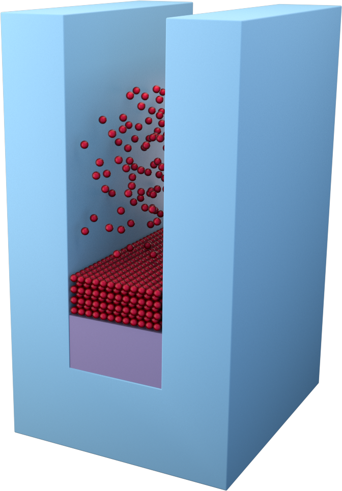
ALD has emerged as a crucial technology, particularly for front-end processes, allowing for highly controlled thickness at the atomic scale. While not new, its relevance has grown as dimensions shrink to a point where atomic counts become critical. ALD’s self-limiting surface reactions enable uniform layer formation, especially in challenging geometries.
This precision makes ALD indispensable for developing high-k dielectrics and barrier films, essential for modern transistors operating under high electrical demands. Victor Moroz from Synopsys highlights ALD’s importance for gate-all-around structures, where thick dielectric layers must be deposited with extreme uniformity.
However, ensuring uniformity is essential; small variations in ALD thickness can lead to significant issues across billions of transistors. Simulation technology is proving valuable for exploring deposition behaviors, yielding faster iterations in design and ensuring proper material application.
Emerging Strategies and Hybrid Solutions
As complexity rises, deposition strategies continue to evolve, incorporating techniques like sputter epitaxial growth, which allows precise thickness control for larger areas. ALD remains dominant for conformal structures, but its slower growth rates mean hybrid approaches are increasingly common. This balancing act of stress and conformality is critical, particularly in modern semiconductor fabrication where mechanical stability is paramount.
Given the various materials required for front-end and back-end processes, manufacturers must ensure that each layer maintains the desired properties while mitigating integration risks. Collaboration between stakeholders is more vital than ever, with early-stage material selection becoming essential to prevent issues further down the production line.
The mechanical behavior of increasingly thin films also poses new challenges. Combining ALD with other methods like plasma-enhanced chemical vapor deposition enhances overall material performance while addressing mechanical concerns like stress. These hybrid systems effectively integrate mechanical stability with electrical functionality.
Precision Control and Reliability Challenges
As manufacturing techniques hone in on atomic precision, process control becomes increasingly critical. Real-time monitoring embedded in reaction processes helps maintain adherence to strict uniformity standards. Machine learning and advanced simulations further enhance understanding and management of layer interactions.
Reliability hinges not just on the films themselves but on their interfaces. As designs grow thinner, ensuring adhesion and eliminating defects are crucial to preventing failures. The interactions between layers are integral to the system’s overall robustness.
Future Directions
The semiconductor industry is evolving toward hybrid dielectric integration, blending ALD and traditional deposition methods to achieve optimal performance and reliability. Technologies are being customized to meet the needs of advanced packaging and integration, ensuring systems can handle the demands of next-gen AI architectures.
As semiconductor advancement shifts focus from merely shrinking features to innovating materials, collaboration across the supply chain will be critical. The continual integration of advanced dielectrics, bolstered by precise engineering, will define the next frontier in semiconductor performance.
The content above is a summary. For more details, see the source article.


