Key Takeaways
- A range of innovative methodologies are enhancing photonic integrated circuits (PICs).
- Recent advancements include high-speed laser lithography and machine-learning applications in lithography processes.
- These developments aim to improve precision and efficiency in semiconductor manufacturing and nanofabrication.
Advancements in Photonic Integrated Circuits
Recent studies highlight significant progress in photonic integrated circuits (PICs), which play a crucial role in optical communication and sensor technologies. Innovations in this field are addressing challenges related to efficiency, speed, and precision.
One notable development is the introduction of a photonic-electronic integrated circuit-based coherent LiDAR engine by Lukashchuk et al. This engine promises enhanced sensing capabilities for various applications, including autonomous driving and environmental monitoring. The integration of photonic and electronic components allows for better signal processing and improved measurement accuracy.
Additionally, a hybrid architecture combining reinforcement learning with PICs has been demonstrated. Research led by Li et al. showcases how machine learning algorithms can optimize the design and efficiency of photonic systems, paving the way for smarter and faster processing capabilities. This approach contributes to the broader trend of implementing artificial intelligence in photonics to streamline manufacturing processes.
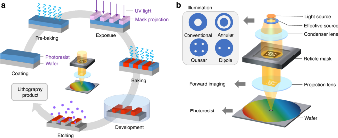
Researchers also report advancements in lithography techniques, particularly in high-speed laser lithography using ultrahigh-printing-speed photoresists. Liu et al. emphasize the potential for improving large-area fabrications, which are essential for various technology sectors, including consumer electronics.
Moreover, novel methodologies such as crosslinking-induced patterning of metal-organic frameworks (MOFs) have been explored. This technique, highlighted by Tian et al., offers a way to develop intricate structures using advanced printing technologies. With direct laser processing, this method opens up new possibilities for creating complex nanostructures used in optical devices.
The ongoing research into 3D electron-beam writing at sub-15 nm resolution, as noted by Qin et al., is setting the stage for breakthroughs in nano-fabrication. This precision will allow for the creation of more sophisticated photonic devices.
Environmental considerations are also at the forefront, with Liu et al. reporting the development of biomimetic sapphire windows, created through unique laser processes. These windows hold promise for applications in protective optics, potentially reducing manufacturing costs and time.
Overall, advancements in photonic integrated circuits and related technologies continue to evolve. From innovative laser lithography to the application of machine learning, these developments are crucial in shaping the future of electronics and integrated photonics, ultimately enhancing capabilities in telecommunications, autonomous systems, and environmental sensing.
The content above is a summary. For more details, see the source article.