


Key Takeaways
- Researchers from Peking University developed a method to integrate 2D semiconductors with dielectric materials, enhancing electronic performance.
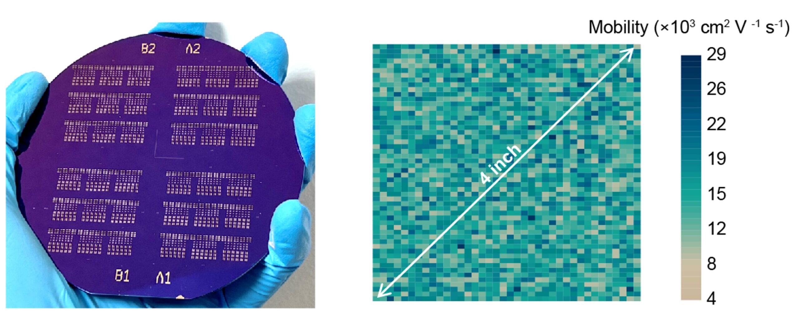
- The new technique ensures minimal defects during the transfer of a 4-inch graphene wafer, preserving its intrinsic electrical properties.
- This approach may lead to scalable low-power microelectronics and advancements in 3D integration of 2D materials.
New Method for Integrating 2D Semiconductors
Recent advances in semiconductor technology have highlighted the potential of two-dimensional (2D) materials in creating smaller yet highly efficient electronic components. While substantial progress has been made in synthesizing these materials, their effective application in devices has faced challenges, particularly regarding the transfer and integration processes.
A team of researchers from Peking University and the Beijing Graphene Institute has introduced a novel method to facilitate the integration of 2D semiconductors with dielectric materials. This method, detailed in a paper published in Nature Electronics, revolves around the epitaxial growth of an ultra-thin dielectric film on a graphene-covered copper surface. This innovative process minimizes defects during the transfer of 2D materials onto various substrates.
The lead authors of the study, Zhongfan Liu, Li Lin, and Yanfeng Zhang, emphasized the prevalent issues associated with traditional transfer methods. Conventional techniques often involve polymer supports that can introduce contamination, mechanical stress, and defects at the interface, which ultimately degrade device performance. Their paper addresses these challenges by proposing a comprehensive, wafer-scale process that retains the intrinsic properties of graphene while ensuring a clean interface during transfer.
In demonstrating their process, the researchers synthesized a single-crystal dielectric material, specifically antimony oxide (Sb2O3), which is deposited on graphene grown atop a Cu(111) substrate. Li Lin explained that the vacuum thermal evaporation process was employed to achieve the epitaxial growth of Sb2O3 on graphene. By pre-treating the copper substrate with a water-ethanol mixture, they created a thin oxide layer that decreases adhesion between the graphene and copper, facilitating a smoother transfer.
The outcome of their method was notable; it allowed for the reliable transfer of a 4-inch graphene wafer with minimal defects. The preservation of graphene’s electrical properties was evident, with an average carrier mobility recorded at approximately 14,000 cm2 V-1 s-1. Furthermore, the resultant devices exhibited exceptional uniformity and long-term stability, with only minor performance variations even after prolonged air exposure.
The implications of this research are substantial, as the proposed technique could significantly enhance the production of high-performing, low-power microelectronics and optoelectronics that utilize 2D materials. Looking ahead, the researchers plan to refine their approach to extend its capabilities into the 3D integration of 2D materials within real devices.
Lin expressed a desire to develop advanced transfer techniques that would facilitate the stacking and precise alignment of 2D materials to create multi-layer, three-dimensional integrated structures. This future research aims to tackle challenges concerning interlayer coupling, interface control, and patterning in 3D configurations, thereby paving the way for the fabrication of high-performance, densely integrated electronic and optoelectronic devices.
The content above is a summary. For more details, see the source article.


