


Key Takeaways
- Harvard researchers developed a silicon chip that records signals from over 2,000 rat neurons, mapping 70,000 synaptic connections.
- The University of Chicago created a memory device using atomic crystal defects, capable of storing terabytes of data in a cubic millimeter.
- Korean researchers deployed a real-time measurement system to diagnose the lifespan of semiconductor plasma equipment, preventing contamination from corrosion.
Innovative Technologies in Neuroscience, Data Storage, and Semiconductor Diagnostics
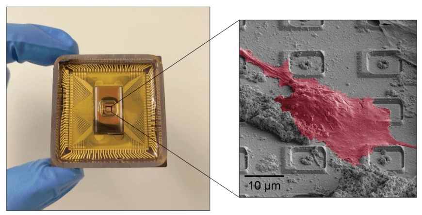
Researchers from Harvard University have made significant strides in understanding synaptic connections by creating a silicon chip that can record synaptic signals from an expansive number of neurons. This new device has successfully catalogued over 70,000 synaptic connections from approximately 2,000 rat neurons, paving the way for a detailed synaptic connection map of the brain. The chip features an array of 4,096 microhole electrodes, which function similarly to the established patch-clamp electrodes but allow for simultaneous multi-neuron recordings.
Woo-Bin Jung, a researcher involved in the project, emphasizes the importance of the chip’s integrated electronics, which facilitate gentle current delivery and simultaneous recording of intracellular signals. Remarkably, around 90% of the electrodes were effectively coupled to neurons, greatly enhancing the team’s data collection capabilities compared to earlier models that utilized nanoneedles. This effective data collection has resulted in the categorization of synaptic connections based on their characteristics and strengths. Donhee Ham, a Harvard engineering professor, highlighted the challenge of analyzing the resulting large data set but confirmed that progress is being made toward a more sophisticated design that could be applied in live brain studies.
In a separate breakthrough, researchers at the University of Chicago have developed a novel technique to store vast amounts of data using atomic defects in crystal structures. By incorporating Praseodymium ions into an Yttrium oxide crystal and stimulating them with an ultraviolet laser, researchers can manipulate the electronic states of the crystal defects to serve as memory cells. Each defect represents a single memory unit, allowing the device to pack terabytes of data into a tiny millimeter-sized cube. This innovative approach utilizes the natural defects in crystals as a means of storing information, vastly increasing data density.
Additionally, a collaboration between researchers from Korea Research Institute of Standards and Science, Hanyang University, and SK Hynix has led to the creation of a real-time measurement system designed to assess the lifespan of components used in semiconductor plasma processing. This system addresses the challenges posed by contaminant particles generated from the corrosion of equipment, which can compromise wafer quality and process performance. By analyzing the film peeled off from components in the plasma environment, the system can detect fine particles in real-time, providing immediate diagnostic information regarding the remaining lifespan of parts. This advancement serves as a valuable testing ground for manufacturers of semiconductor equipment and components in Korea.
These innovations across neuroscience, data storage, and semiconductor diagnostics highlight the ongoing advancements in technology and research that promise significant applications in various fields.
The content above is a summary. For more details, see the source article.


