Key Takeaways
- Advanced packaging is shifting from chiplet-focused designs to integrated systems, enhancing performance and efficiency.
- Technologies like antenna-in-package and co-packaged optics are enabling innovations in wireless communication and data transmission.
- As advanced packaging evolves, it paves the way for sophisticated, multifunctional devices in various fields, from IoT to biomedicine.
Transforming Semiconductor Packaging
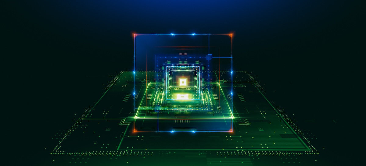
In recent years, advanced packaging has risen in prominence, as semiconductor manufacturers are shifting their focus from simply miniaturizing chips to optimizing entire systems. The goal is to seamlessly integrate processor cores, memory, sensors, and wireless components into a single housing, enhancing performance and energy efficiency.
While chiplets, which break down complex systems into smaller, specialized components, remain significant, advanced packaging encompasses much more. This new design approach merges mechanical, electrical, thermal, and optical elements, allowing engineers to create systems that are more powerful, energy-efficient, and reliable.
Innovations in Integration
Modern packaging technologies aim to maximize functionality and minimize signal paths without sacrificing performance. Techniques such as through-silicon vias (TSVs), 2.5D interposers, and fan-out wafer-level packaging enable the stacking or close integration of multiple active chips. This tight coupling facilitates improved power supply, heat dissipation, and communication between functional units.
Combining diverse technologies—like logic, memory, and sensors—within one package results in high-performance, heterogeneous systems that occupy minimal space. Additionally, this approach reduces cabling, leading to faster data transmission and less signal loss.
Next-Generation Wireless Technologies
A prominent application of advanced packaging is in high-frequency and antenna technologies, particularly with the shift to millimeter wave and sub-THz bands. Antenna-in-package (AiP) solutions allow for compact antennas integrated directly into the package, supporting applications such as 5G and future 6G technologies.
The demand for multiple antennas within a single module, necessary for beamforming and multi-channel transmission, makes advanced packaging essential. The precision and integrity it provides in antenna structures support the development of compact Internet of Things (IoT) devices, autonomous vehicles, and satellite systems where space and energy efficiency are critical.
Optical Data Transmission
Advanced packaging is also crucial for future optical data transmission. As data rates in high-performance computing and data centers increase, traditional electrical interfaces are becoming inadequate. Co-packaged optics (CPO) integrates optical transceivers within the same package as processing units, lowering signal paths and enhancing energy efficiency.
Combining silicon photonics with CMOS electronics is expected to form the basis for high-performance architectures, delivering rapid data rates while reducing power consumption significantly.
Advanced Sensors and Integrated Systems
Beyond high-performance electronics, advanced packaging opens new avenues in sensor technology. Microelectromechanical systems (MEMS) sensors are evolving to become smaller and more sensitive. Integrating various sensor elements with processing electronics enables sophisticated platforms capable of real-time data processing.
Innovative packaging allows direct connections for sensor elements via TSVs and backside contacts, eliminating the need for contact pads. This level of integration is vital for applications in quantum optics, LiDAR, biomedicine, and autonomous systems, leading to the development of smaller and more powerful sensor modules.
The Road Ahead
As advanced packaging becomes integral to the electronics industry, the lines between chip design, assembly, and system architecture are blurring. Future innovations will stem from the intelligent integration of functional components rather than just advances in individual transistors.
The groundwork laid by advanced packaging is essential for the next generation of connected, energy-efficient, and multifunctional systems. Companies that adopt these technologies early will secure a competitive edge in shaping future electronics architectures.
The content above is a summary. For more details, see the source article.