


Key Takeaways
- Interposers and substrates are transitioning from intermediaries to engineered platforms crucial for performance in AI and high-performance computing.
- Emerging materials like organic and glass substrates address limitations of traditional silicon interposers, enabling higher density interconnects and improved thermal management.
- Advancements in hybrid bonding and active interposer designs are setting the stage for smarter packaging, enhancing efficiency and reliability in next-generation semiconductor applications.
Transforming Semiconductor Packaging
Interposers and substrates are undergoing a significant evolution as they shift from passive roles to active components in advanced computing systems. This transformation is driven by the growing demands of artificial intelligence (AI), high-performance computing (HPC), and next-generation communication technologies. As these fields require higher performance and integration densities, traditional printed circuit board (PCB) technologies, which maintain line widths of 20 to 30μm, fall short against the rapidly shrinking transistor sizes in the single-digit nanometer range.
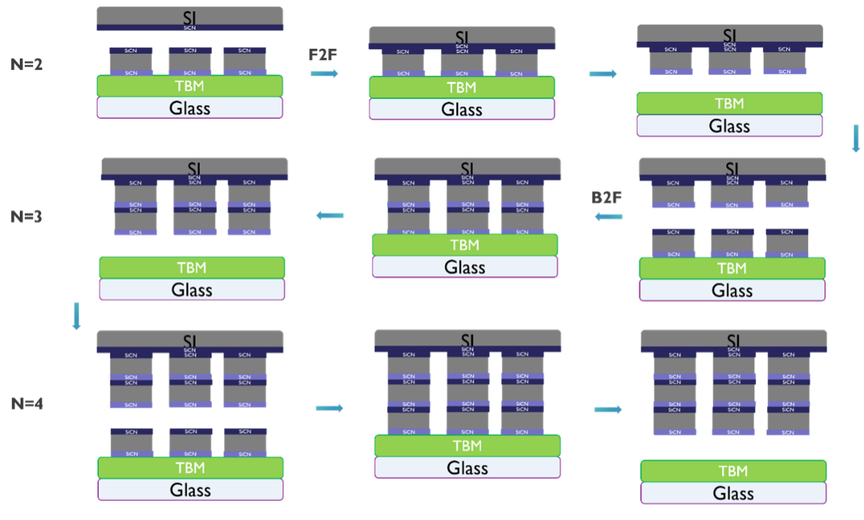
The limitations of conventional packaging have created a bottleneck, prompting the evolution of interposers and advanced substrates to meet new standards, including incredibly fine redistribution layers (RDLs) of 1 to 2μm and innovative hybrid bonding techniques. The industry is increasingly favoring organic and glass substrates over traditional silicon interposers because these materials facilitate larger chiplet architectures and denser interconnects.
According to Dick Otte, CEO of Promex, adapting quickly to novel substrate materials and bonding methods is now essential for maintaining manufacturing efficacy. As the demand for higher interconnect densities escalates, deploying new substrate materials becomes crucial.
Bridging the Interconnect Gap
Redistribution layers have long been fundamental in connecting signals between integrated circuits. However, as the complexity of packaging escalates, demands on RDL technology also increase. The semiconductor industry is witnessing a significant shift from silicon to organic and glass interposers, which allow for greater scalability while improving robustness and interconnect density.
Chee Ping Lee, managing director for advanced packaging at Lam Research, highlights that the push for larger, more efficient substrates must address challenges related to warpage control, defect detection, and uniform plating processes. Moreover, the shift towards more rectangular glass carriers is enhancing handling and processing efficiency.
As technologies evolve towards fan-out panel-level packaging (FOPLP), the benefits include cost-effective integration of numerous chips on substantial panels, although challenges remain in manufacturing yield and process control.
Addressing Manufacturing Challenges
Manufacturing precision at the nanoscale remains a critical issue for substrates and interposers, particularly as interconnects become finer and more intricate. Fabricators must ensure that die placement remains accurate, as even minor misalignments can severely impact electrical performance and reliability.
Thermal management within advanced packaging continues to be a significant concern due to increased power densities and heat generation. Consequently, manufacturers are exploring integrated thermal pathways, such as embedded microfluidic cooling channels and new thermal interface materials, as effective solutions.
New material innovations, including glass-core substrates, are gaining traction for their beneficial dielectric properties and temperature stability, although they still face challenges in manufacturing processes such as precision laser drilling and material brittleness. The incorporation of hybrid substrates is also on the rise, combining the strengths of different materials to push the limits of performance while managing thermal expansion mismatches.
New Bonding Technologies
As the industry evolves, existing micro-bump bonding strategies reveal limitations in meeting the increased demands for fine-pitch interconnections. Hybrid bonding techniques are now being adopted, enabling sub-10μm interconnect pitches through advanced dielectric bonding methods.
The move towards direct copper interconnects further enhances electrical performance but brings its own set of manufacturing challenges. To navigate these complexities, manufacturers are harnessing AI-driven process control and simulation technologies to maintain high yields.
Lastly, as substrates diverge from traditional designs, the application of AI in predictive modeling and defect detection is proving essential for ensuring seamless integration and reliability in next-generation semiconductor packaging architectures.
In summary, as interposers and substrates evolve into sophisticated components of computing systems, new materials, manufacturing techniques, and intelligent designs are reshaping the semiconductor landscape, opening the door for superior performance, efficiency, and reliability in the next generation of chiplet-based computing solutions.
The content above is a summary. For more details, see the source article.


