


Key Takeaways
- Northrop Grumman’s Microelectronics Center is advancing diamond-based technologies for microelectronics, demonstrating exceptional durability for military applications.
- Recent tests revealed diamond receivers can handle over 100 Watts of power, surpassing existing semiconductor materials like silicon and gallium nitride (GaN).
- Ongoing research aims to upscale diamond technology for compact, energy-efficient systems suitable for future combat scenarios.
Groundbreaking Developments in Diamond-Based Microelectronics
Research at Northrop Grumman’s Microelectronics Center (NGMC) is revolutionizing the understanding of diamonds as advanced materials for microelectronics. As the demand for more resilient solutions rises amidst evolving military challenges, diamonds have emerged as a potential game-changer in semiconductor technology.
Diamonds possess unique features that make them ideal for high-performance electronics:
– They endure extreme temperatures without degradation.
– Their thermal conductivity outperforms copper by a factor of five.
– They effectively manage high power loads.
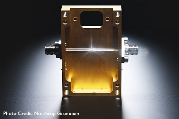
In a recent breakthrough, Northrop Grumman successfully tested a diamond-based receiver-protection component that sustained over 100 Watts of power, more than double the current capabilities of conventional devices. These micro-engineered diamonds, much smaller than traditional gemstones, exhibit remarkable electronic and thermal properties, vital for shielding systems from power surges and excessive heat while maintaining signal clarity.
Dr. Ugonna Ohiri, a staff systems engineer at the NGMC, noted: “The exceptional thermal conductivity and mobility that diamond possesses allow the material to perform well in very high temperatures.” Diamonds are proving to be a robust alternative to traditional semiconductor materials such as silicon and gallium nitride (GaN).
Since beginning diamond development in 2019, Northrop Grumman’s team has transitioned research from a small lab into a cleanroom environment, demonstrating promising capabilities and securing vital partnerships. The diamond wafers being produced are minuscule, measuring just 1 x 1 mm, yet can yield even smaller chips for sophisticated applications, including space missions and airborne platforms. This compact design supports reduced weight and power consumption while delivering high-level performance.
Furthermore, the strategy to scale this technology involves collaboration with Arizona State University’s Southwest Advanced Prototyping Hub (SWAP), as part of the Microelectronics Commons initiative. This partnership aims to produce larger diameter diamond wafers, enhancing the ability to meet future military needs effectively.
Reflecting on the potential of diamond materials, Dr. Ohiri remarked, “The sky isn’t the limit—the universe is.” As research progresses, the transition of diamond technology from concept to widespread application appears imminent, confirming its status as the next-generation solution in semiconductor manufacturing.
The content above is a summary. For more details, see the source article.


