

Key Takeaways
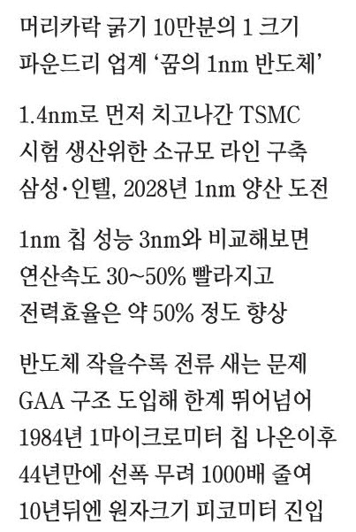
- Semiconductor companies, including TSMC and Samsung, are preparing for the production of 1nm chips, with expectations for testing by 2027.
- The shift to 1nm technology could significantly enhance device performance, increasing speed by 30-50% and energy efficiency by 50% compared to 3nm chips.
- Nvidia aims to leverage 1nm chips for its upcoming “Feynman Architecture” GPU, promising a dramatic increase in computational performance.
The term “nano,” derived from the Greek word for “dwarf,” describes scales at one billionth of a meter. In semiconductor technology, the pursuit of 1nm chips remains an ambitious goal, as 1nm represents an immense reduction from current standards. TSMC has begun preparing for 1.4nm test production, targeting commercial production in 2028, while both Samsung and Intel have laid out their own 1nm development plans.
The promise of 1nm chips lies in their increased transistor density. Transistors act as electrical switches within integrated circuits (ICs), with the potential to revolutionize how devices process information. Current technology allows for billions of transistors to be integrated into tiny ICs, exemplified by Apple’s A16 Bionic chip, which employs TSMC’s 4nm processing technique. Transitioning to 1nm technology could triple transistor density to an estimated 300 million transistors per square millimeter, significantly enhancing performance and energy efficiency.
For example, 1nm chips are projected to operate 30-50% faster and use 50% less energy compared to their 3nm counterparts. These advancements will support improved smartphone capabilities, extended battery life, and accelerated AI model performance. The business model of the semiconductor industry focuses on design firms collaborating with foundries to produce chips, typically creating up to 500 chips from a single 4nm wafer. As chip sizes decrease, more can be produced, albeit at an increased cost—the projected price for 1nm wafers is around $50,000.
Nvidia has sparked competition in the 1nm arena, announcing plans for the “Feynman Architecture” GPU, expected to be manufactured using 1nm technology. This new architecture could boast performance enhancements to between 15 and 20 PFLOPS, surpassing current models. To achieve this, companies are addressing challenges like current leakage in miniaturized transistors. Samsung has steps forward with a gate-all-around (GAA) structure in its 3nm technology, while other competitors will implement similar strategies aimed at maintaining transistor performance.
The future of semiconductor technology is bright, though it involves ongoing research into advanced equipment and materials. Major players like TSMC aim to maintain their market share while developing next-generation chips in Taiwan. As progress continues and demands evolve, it is anticipated that 1nm semiconductors will begin appearing in consumer devices around 2027, marking a significant step in the evolution of chip technology.
The journey from the first 1-micrometer chip in 1984 to the potential 1nm chips represents a monumental leap in the field. As industry leaders like Intel and Samsung work diligently toward this goal, the semiconductor sector will likely evolve dramatically in the upcoming years, pushing the boundaries of technology.
The content above is a summary. For more details, see the source article.